News
Our products are exported to over 30 countries.
Possess the full-process development capability from concept design to mass production and implementation
In integrated circuit (IC) manufacturing, photolithography is the critical process determining device performance and yield, accounting for approximately one-third of total wafer processing costs. Its technical level directly impacts chip integration density and reliability.
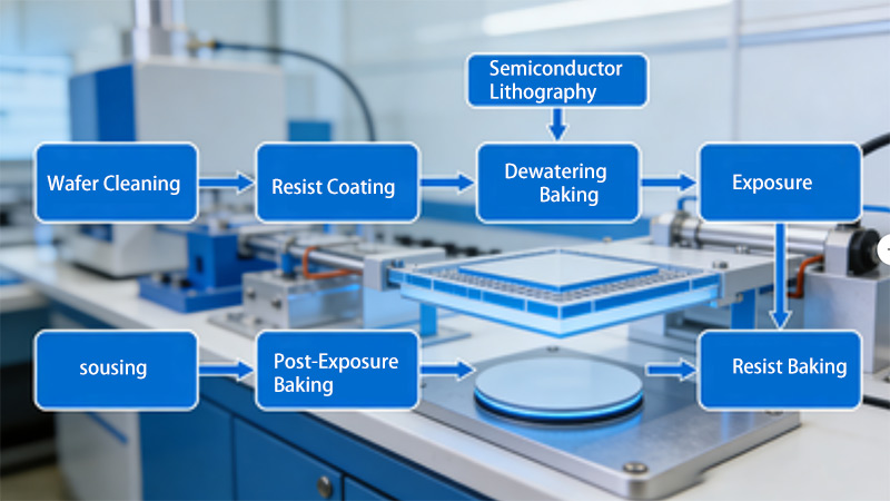
The core of photolithography involves precisely transferring mask patterns onto wafer surfaces through three main steps: resist coating, exposure, and development. "Baking" serves as an auxiliary process throughout this workflow. While not directly involved in pattern transfer, baking optimizes the photoresist's physical and chemical properties by controlling temperature and time, making it essential for ensuring photolithography effectiveness. Professional semiconductor baking lines serve as the core supporting infrastructure.
This article, in conjunction with our company's semiconductor baking line solutions, systematically analyzes the functional mechanisms of baking processes, parameter influences, and equipment advantages, providing valuable reference for enterprise process optimization and equipment selection.
In photolithography, baking occurs at multiple critical stages, decisively influencing pattern quality. Our semiconductor baking lines seamlessly adapt to each stage's requirements, achieving precise alignment between process and equipment.
After cleaning and before photolithography, wafers undergo Dehydration Bake (150-200°C, several seconds to minutes). This step removes surface moisture molecules, enhancing photoresist adhesion and coating uniformity. Our baking lines feature high-precision temperature control modules with ±1°C fluctuation. The closed-loop heat conduction design ensures temperature uniformity, perfectly adapting to dehydration baking needs for various wafer specifications.
Following resist coating, Soft Bake (Post-Apply Bake, 90-120°C, 30-60s) is required. Its purpose is to remove photoresist solvents, eliminate internal stress, prevent contamination of equipment from volatilization, and improve exposure resolution. Our baking lines optimize the hotplate conduction structure using highly thermally conductive materials. Temperature can be flexibly adjusted based on photoresist type and thickness, precisely controlling solvent content to ensure process stability.

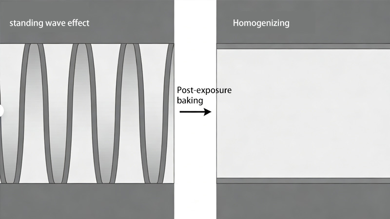
After exposure, Post-Exposure Bake (PEB) is necessary to mitigate standing wave effects caused by optical interference, resulting in clearer pattern edges. The principle involves using thermal energy to promote uniform diffusion of photoactive compounds, optimizing photoresist component distribution. Our baking lines feature intelligent temperature gradient adjustment, support single-wafer independent baking, and allow flexible parameter tuning based on exposure conditions, effectively reducing standing wave effects and enhancing resolution.
After development, Hard Bake (Post-Develop Bake) is conducted. Its core functions are evaporating residual photoresist solvents, curing the resist film, enhancing adhesion to withstand subsequent ion implantation or etching processes, and ensuring pattern stability. Our baking lines support a wide temperature control range, thoroughly removing residual solvents, increasing resist film hardness, reducing pattern deformation or peeling, and safeguarding chip yield.

In summary, our semiconductor baking lines fully adapt to all four core baking stages in photolithography. With precise temperature control and flexible parameter adjustment, they provide robust support for process quality.
(1) Specific Manifestations of Full-Process Adaptability
Adaptability is reflected in three dimensions: "All Stages, All Specifications, All Scenarios." First, compatibility with all four baking stages allows completion of each step without equipment changes. Second, compatibility ranges from inch-scale to 12-inch wafers, meeting different photoresist parameter requirements. Third, switchable single-wafer and batch baking modes with software-based parameter adjustment adapt to diverse production scenarios.
(2) Core Impact of Full-Process Adaptability on Production Efficiency
Enhances Production Continuity: Eliminates the need for multiple separate equipment purchases, avoiding wafer transfer time and loss, accelerating production cycle time.
Reduces Setup Costs: Enables quick calling of preset parameters, shortening process switchover time, minimizing rework rates.
Increases Unit Output: Automated linkage design reduces manual intervention, while low failure rates ensure continuous operation, meeting large-scale production demands.
Semiconductor baking primarily utilizes hotplates (conduction heating) or ovens, with hotplates offering higher precision. Traditional hotplates transfer wafers via lift pins, use vacuum adsorption, and conduct heat to the wafer for baking.
Our baking lines upgrade traditional technology with a "Hotplate Conduction + Precision Temperature Control + Intelligent Linkage" design. Highly thermally conductive materials minimize heat radiation loss, adhering to Fourier's Law to ensure uniform heat conduction.
Semiconductor baking equipment requires PID temperature control systems for closed-loop feedback. Our integrated high-precision PID system improves response speed by 30%, achieving temperature control accuracy of ±0.5°C, exceeding industry standards.
Core Advantages of Our Semiconductor Baking Line:
Full-Process Adaptability, compatible with multiple wafer specifications and production modes.
Temperature Control Accuracy of ±0.5°C, ensuring process stability.
Automated Linkage for high efficiency and low failure rates.
Flexibly Adjustable Parameters to meet personalized requirements.
Intelligent Operation and Maintenance, reducing operational costs.
As a professional semiconductor oven manufacturer, we provide customized solutions to help enterprises optimize processes, improve yields, reduce costs, and support the high-quality development of semiconductor manufacturing.
19 years of focus on research and development as well as production